

Announced at the Seaholm Power Plant in Austin, Texas, the Terafab concept seeks to consolidate the entire semiconductor manufacturing lifecycle within a single, hyper-automated physical footprint.
The modern semiconductor industry operates on a highly segmented global supply chain.
Silicon wafers are often designed in Silicon Valley, fabricated in Taiwan or South Korea, packaged in Malaysia, and finally integrated into products worldwide. The Tesla Terafab, a joint venture uniting Tesla, SpaceX, xAI, and Intel, represents a radical departure from this fragmented model.
<script async src="https://pagead2.googlesyndication.com/pagead/js/adsbygoogle.js?client=ca-pub-3829624412957312"
     crossorigin="anonymous"></script>
<ins class="adsbygoogle"
     style="display:block; text-align:center;"
     data-ad-layout="in-article"
     data-ad-format="fluid"
     data-ad-client="ca-pub-3829624412957312"
     data-ad-slot="2552026584"></ins>
<script>
     (adsbygoogle = window.adsbygoogle || []).push({});
</script>
Designed to produce an unprecedented 1 terawatt of artificial intelligence compute capacity annually, the project aims to solve the severe semiconductor bottleneck threatening the mass production of autonomous vehicles, humanoid robotics, and space-based compute nodes.
Announced at the Seaholm Power Plant in Austin, Texas, the Terafab concept seeks to consolidate the entire semiconductor manufacturing life-cycle within a single, hyper-automated physical footprint.
Designed to produce an unprecedented 1 terawatt of artificial intelligence compute capacity annually, the project aims to solve the severe semiconductor bottleneck threatening the mass production of autonomous vehicles, humanoid robotics, and space-based compute nodes.
Architectural Concept: End-to-End Vertical Integration
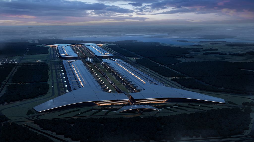
At its core, the Terafab is built on total vertical integration. Rather than outsourcing specialized sub-processes, the facility is designed to execute every stage of semiconductor manufacturing under one massive roof:
- Integrated Chip Design & Photomasking: On-site iteration of circuit designs and high-precision photomask templates.
- Front-End Fabrication: Advanced silicon wafer processing using sub-2nm nodes.
- Memory Production: Localized manufacturing of high-bandwidth memory (HBM) and storage architectures.
- Advanced Packaging & Testing: High-density 2.5D and 3D multi-chip module integration prior to field deployment.
[Raw Materials / Wafers]
         │
         ▼
 ┌───────────────┐
 │ Photomasking  │ ◄─── Fast Recursive Design Loop
 └───────┬───────┘
         │
         ▼
 ┌───────────────┐
 │ Fabrication   │ (Intel 14A / Sub-2nm Process)
 └───────┬───────┘
         │
         ▼
 ┌───────────────┐
 │ Memory / Packaging & Testing │
 └───────┬───────┘
         │
         ▼
[Compute Output: Autonomous Vehicles, Optimus, Orbital AI]
By removing international transport delays, supply chain tariffs, and cross-company hand-offs, the facility introduces a tight feedback loop.
Design adjustments identified during advanced packaging tests can immediately update the on-site photo-mask equipment.
The primary physical site in Grimes County, Texas, is engineered to cover approximately 100 million square feet across a 2.5-mile footprint—making it potentially the largest single industrial building by floor area on Earth.
<script async src="https://pagead2.googlesyndication.com/pagead/js/adsbygoogle.js?client=ca-pub-3829624412957312"
     crossorigin="anonymous"></script>
<ins class="adsbygoogle"
     style="display:block; text-align:center;"
     data-ad-layout="in-article"
     data-ad-format="fluid"
     data-ad-client="ca-pub-3829624412957312"
     data-ad-slot="2552026584"></ins>
<script>
     (adsbygoogle = window.adsbygoogle || []).push({});
</script>
The complex is planned to operate as a self-contained “industrial city,” utilizing high-density automated transit corridors designed specifically for autonomous transport robots rather than human foot traffic.
To satisfy its extreme power footprint, initial infrastructure plans include dedicated high-capacity natural gas generation supplemented by utility-scale Mega-pack battery storage.
Key Technological Drivers
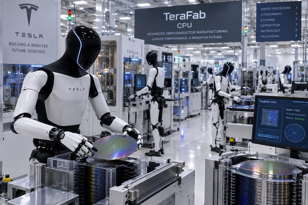
The custom silicon produced within the Terafab is targeted toward two major end-use domains:
- Edge Compute for Autonomous Robotics: High-yield inference chips optimized for low latency and high power efficiency, built to power millions of Tesla Full Self-Driving (FSD) vehicles and Optimus humanoid robots.
- Radiation-Hardened Space Silicon: Specialized compute units explicitly engineered to withstand cosmic radiation, extreme thermal cycles, and electron buildup for SpaceX’s satellite constellations and deep-space infrastructure.
Through its partnership with Intel, the facility leverages Intel’s 14A (1.4nm) process node alongside advanced glass-substrate packaging technologies. This allows the venture to skip several intermediate nodes and immediately target next-generation transistor densities.
Project Phasing and Estimated Timelines
Building a multi-billion-dollar semiconductor mega-factory requires a staggered, multi-phase execution strategy. The total projected outlay ranges between $55 billion and $119 billion across all build phases.
| Phase / Facility | Primary Focus | Capital Commitment | Target Milestone | Status |
| Austin ATCF (Prototype) | R&D, small-scale pilot cleanroom, equipment testing | ~$3 Billion | First prototype silicon wafer runs | Groundbreaking complete; active foundation work |
| Grimes County Phase 1 | Primary fab shell, basic cleanrooms, gas power plant installation | $16.8 Billion | Construction start late 2026; shell complete by 2028 | Permits & tax abatement agreements approved |
| Grimes County Phase 2–4 | Full 100M sq ft scale-out, memory lines, 1 TW total compute capacity | ~$35B–$100B+ | Staggered activation through 2030s | Long-term planning & zoning |
- Pilot Operations: Physical construction began at Tesla’s Giga Texas North Campus for the Advanced Technology Chip Fabrication (ATCF) pilot line. This site serves as a sandbox for refining automated wafer movement and tuning lithography tools before scaling up.
- Commercial Ramp: Construction on the main Grimes County mega-factory is slated to break ground in late 2026, with the initial structure projected to reach clean room readiness by 2028. Full operational capacity across all four planned phases is scheduled to scale progressively throughout the 2030s.
Engineering Challenges Ahead
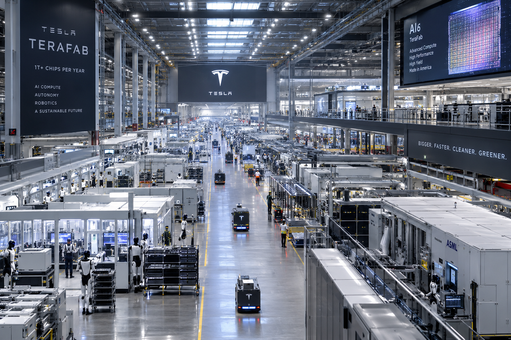
While the Terafab presents a compelling vision for domestic advanced manufacturing, its complexity carries substantial risk.
<script async src="https://pagead2.googlesyndication.com/pagead/js/adsbygoogle.js?client=ca-pub-3829624412957312"
     crossorigin="anonymous"></script>
<ins class="adsbygoogle"
     style="display:block; text-align:center;"
     data-ad-layout="in-article"
     data-ad-format="fluid"
     data-ad-client="ca-pub-3829624412957312"
     data-ad-slot="2552026584"></ins>
<script>
     (adsbygoogle = window.adsbygoogle || []).push({});
</script>
Sourcing ultra-pure water supplies, installing state-of-the-art Extreme Ultraviolet (EUV) lithography tools from suppliers like ASML, and achieving commercial wafer yields on new nodes typically take years of tuning.
If successful, the Tesla Terafab will redefine the physical and architectural scale of silicon manufacturing.
By tightly coupling raw silicon processing with AI hardware deployment, it represents one of the most ambitious manufacturing endeavors of the 21st century.
Related posts:
 Elon Musk Net Worth, Fortune, Career & Business Life
 Colonizing Mars For Sustaining Humanity’s Future
 Top 10 Fascinating Facts About the Sun
 Top 10 Oldest Game Consoles by Popularity
 NATO Fortifies Lithuania Eastern Flank with New Defense System
 Russian Panic: The Devastating Impact of Refinery Bombing

